Concept of the LPB Format
The design margin for timing and noise is decreasing due to the higher speed of systems and the low voltage of the interface and power supply. Also, balancing design for both cost and performance is increasingly becoming important for cost competitiveness. In a conventional design, the LSI, package and board (LPB) are designed with margin in accordance with individual design guidelines. However, it becomes difficult to provide design guidelines for each LPB part separately with the decreased design margin. Therefore, deciding the design target needs the cooperation of the designers of each part of the LPB. In other words, the innovation of deciding design guidelines by using simulation technology is needed in the system design process. To perform this task, a rapid and accurate simulation environment is necessary.
Conventional design
In conventional design, LPB design and sign-off analysis were performed for each design criterion. In other words, only partial optimization was done, so whole-system optimization and analysis was not performed at the initial design stage. The result was a lack of observation of physical phenomena throughout the whole system, appropriate design changes on each design site separately, and excessive estimation for design margin. These significantly influenced the quality and cost of the final product.
Common problems at the design site
Misunderstanding among designers
Misunderstanding among designers can occur when the designers use the same word in different meaning. Such things happen very often. The words that designers use regularly depend on the design culture of the organization, so communication between designers from different organizations tend to be misunderstood. This happens even for design documents exchanged between different organizations. Many designers should have the unfortunate experience of such misunderstandings of communication. This is a big issue for LPB interoperable design where many organizations are involved.
Lack of information for system design
Limitations and design margins among the LSI, package and board may not be assumed at the time of the design of the individual components. Also designers may face big obstacles after connecting individual components because they are uncertain about the limitations and margins of the others. For example, designing the package or board (wiring) will be difficult because of lack of information about the LSI pad assignment, the package ball assignment, and the part location on the board.
Waste of time that should be used for design
Because input and output formats are different for each electronic design automation (EDA) vendor, in some cases the designer needs to convert the format at the time of the delivery of the data from the different EDA vendors. Problems occur when the designer lacks information at the time of format conversion and has to make up for its lack later. In addition, the pin name and net names may be different for every LSI circuit, package and board. The designer needs to adjust those data and spend painful time in correction.
Concept of LPB interoperable design
Interoperable design is the solution method for the problems with using conventional individual design methods for each LPB part. It is defined as the style that each LPB section uses to cooperate and design. At first, the designer makes minimum design guidelines to satisfy the product’s performance standards by designing through the whole LPB using the interoperable design. After that, the designer designs each part individually in accordance with the design guidelines. After each individual design is completed, the designer performs a simulation for integrating that part with the whole LPB, confirms the performance of all products, and provides feedback on the designs for all other parts accurately.
Value creation by LPB interoperable design
Effects of LPB interoperable design
LPB interoperable design is an appropriate method of design throughout a whole system for signal integrity and power integrity among LPB components. Use of LPB interoperable design makes it is possible to get the effect described in the following subclauses.
Reduction of development cost and time by design flow without iteration
When the designer finally connects the parts designed by partial optimization, an unexpected lack of design margin sometimes occurs. The designer then needs to discover which part of the LPB is causing the margin bottleneck. As a result, the designer may not only spend a lot of time but also need additional recovery costs for creating the needed design margin. In such cases, it is possible to reduce the development cost and time by starting LSI design, package design and board design with each designer sharing information and cooperating from the point that the LSI design begins. Figure 1 compares conventional design flow and LPB interoperable design flow. The LPB interoperable flow reduces development costs and time.
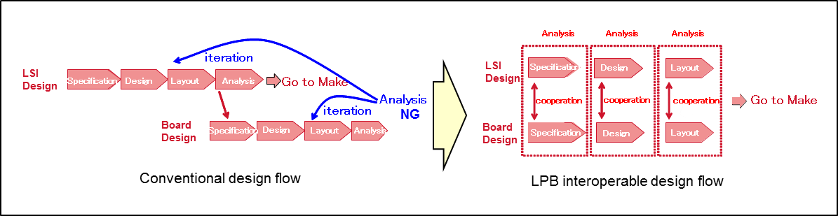
Figure 1 —Conventional design flow versus LPB interoperable design flow
Reduction of system total cost
In conventional design, because a designer designs each part of the LSI, package and board separately with individual margins, the design margin of the product as whole system sometimes becomes excessive when each part are finally connected. It is possible to reduce the total cost using LPB interoperable design because the design margin for the whole design is controlled and held in total, including reduction of the number and cost of the parts used in the design. Figure 2 compares the design margins of conventional design flow and LPB interoperable design flow.
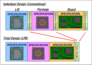
Figure 2 —LPB interoperable design can control design margin
LPB Format
LPB Format solves the problems in conventional design methodologies, improves product quality, and reduces design time. LPB Format is a common language for describing the information required for design and verification. It reduces the preparation time of EDA tools in design teams. Furthermore, LPB can enable the sharing of ideas beyond the design teams. It can become a medium for information distribution in the supply chain. It prevents misunderstanding of design information and improves the information flow in the whole industry. As the result, quality, cost and delivery time (QCD) will be improved.
Summary of LPB Format files
Figure 3 shows one example of how design information is exchanged using the LPB Format. In this example, three types of designers exist: the LSI designer, the package designer and the board designer. All designers exchange design information using LPB Format standard files. By unifying the notation of the files for exchanging design information, it is possible to prevent misunderstandings and to automate the design tool settings.
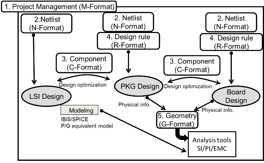
Figure 3 — Example of exchanging design information using the LPB Format
C-Format
The first purpose of C-Format is to give a unified notation to the outer specifications for parts, such as the LSI, package, socket, and so forth. The outer specification is the information needed in order to use the parts, as follows:
- Physical shape of the parts
- Name and type of signal to be input to and output from the parts
- Input/output (I/O) specification, such as the physical shape and position of pins, or swappable pin definitions
- Design constraints, such as the upper limit of the delay or skew
- Design specifications, such as the input impedance of pins or power consumption
By unifying the notation with C-Format, it is possible to exchange information without misunderstanding. For example, a board designer should understand the specifications delivered from several LSI vendors and should set up the design tools based on this understanding. Human error may occur during this process if the specifications are described by each vendor’s own notation. Using C-Format instead of vendor’s own notations, it is possible to set up the design tool automatically and to prevent human error due to misunderstanding. Figure 4 shows an example of the information flow of LSI specifications using C-Format. The LSI specifications are all provided by C-Format even if the vendors are different. The board designer can understand the LSI specifications by reading only one notation, and design tools can automatically set up themselves by entering C-Format.
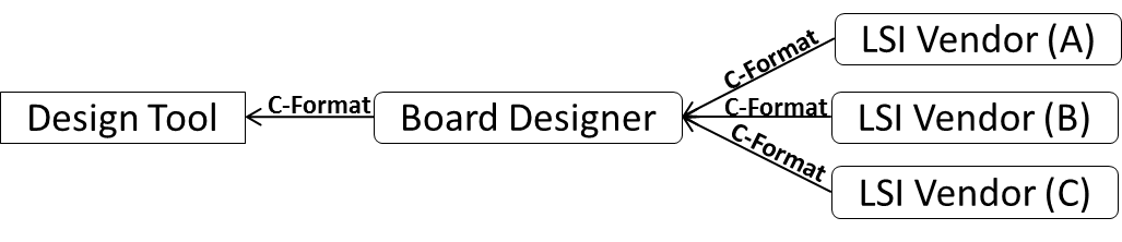
Figure 4 — Example of information flow of LSI specifications using C-Format
Unified notation also smoothly circulates information about specification changes. Figure 5 shows an example of interoperable design flow. A board designer and a LSI designer are collaborating. The information about the pin assignment of the LSI package is provided by the LSI designer. When the board designer want to change the pin assignment of the LSI package, he or she modifies the provided C‑Format file and returns it to the LSI designer. The use of C-Format prevents misunderstanding about the specification change and prevents human error that can occur due to specification changes.
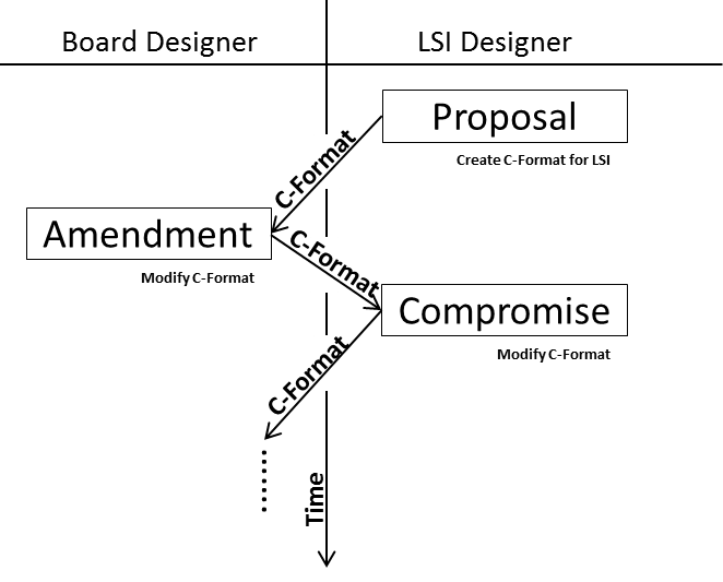
Figure 5 — Example of interoperable design flow with C-Format
The second purpose of C-Format is to provide a unified interface to a simulation model such as a Simulated Program with Integrated Circuit Emphasis (SPICE) netlist, Input/output Buffer Information Specification (IBIS), S-parameters, etc. C-Format wraps these simulation model files and gives cross-references between the nodes of the simulation model and the physical ports of the parts. Simulation tools can plug in the simulation model automatically by entering the wrapped model file. Figure 6 shows an example of exchanging simulation models. Model files are provided with the C-Format file.
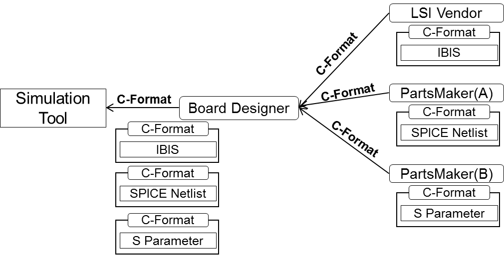
Figure 6 —Example of exchanging simulation models with C-Format
The third purpose of C-Format is to provide connection points to merge multiple layout data. C-Format wraps layout data files, such as Graphic Database System (GDS) II, and gives cross-references between ports in the C-Format file and objects in the layout data file. For example, when the C-Format file wraps a GDS II file, ports in C-Format are associated with the coordinates/layers in the GDS II file. When the C‑Format file wraps a G-Format file, ports in the C-Format file are associated to the pin in the G‑Format file. This feature can be used to merge two or more layout data designed by different design houses. Such situations can occur when the board designer wants to analyze the board with package layout data. The board designer receives the wrapped package layout data from the package designer and enters it in the analysis tools. The analysis tools can find the connection points using the cross-references defined in the C-Format file and merge the layout data of the printed circuit board and the package.
The fourth purpose of C-Format is to support the floorplan of the printed circuit board and package. C‑Format includes placement information about parts. This feature can be used to communicate the floorplan information from the system designer to the board designer. Figure 7 shows an example of design flow when the system designer requests a printed circuit board design to the board designer. At the beginning of the work, the printed circuit board designer can set up the design tools based on the provided C-Format file. By unifying the notation of the floorplan, it is possible to exchange floorplan information without misunderstanding, and to set up the design tool automatically.
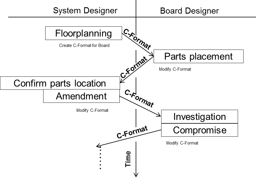
Figure 7 —Example of design flow between system designer and board designer
R-Format
The first purpose of R-Format is to unify the notation of the design rules of the printed circuit board and the package. The following design rules are defined in R-Format:
- Layer stackup of the package and the printed circuit board
- The thickness of the conductive layer/insulating layer
- The material used for each layer
- The material parameters, such as conductivity, dielectric constant, or loss tangent
- Line width and line space
- Via spacing
- Shape of vias
Normally, manufacturers of printed circuit boards and packages provide the design rules using their own notations. The designer has to understand the design rules described in several notations and set up the design tools, with the risk that human error may occur. However, using a unified notation such as R-Format makes it possible to set up the design tool automatically and to prevent misunderstanding. Figure 8 shows an example of exchanging design rules using R-Format. All manufactures provide design rules using the R-Format unified notation. Design tools can set up themselves automatically by entering R-Format.
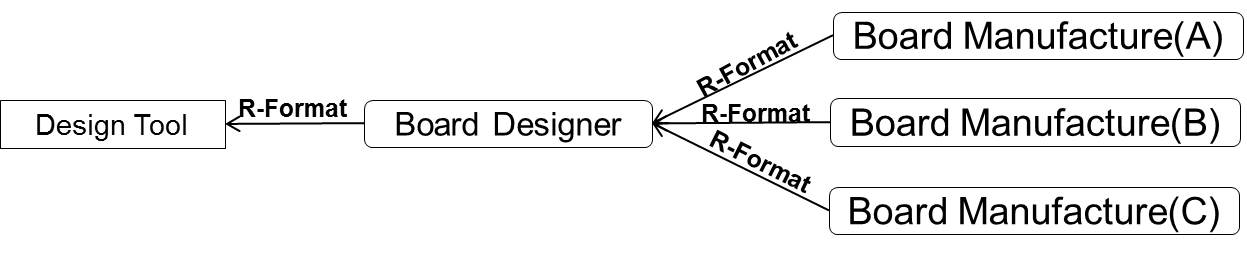
Figure 8 — Example of exchanging design rules with R-Format
The second purpose of R-Format is to define the physical design constraints of the printed circuit board and the package. Where, the physical design constraints mean that the height limitation of mounted parts and non-default design rule area.
G-Format
The purpose of G-Format is to unify the notation of the layout data of the layer stack-up structure, such as the printed circuit board or package. It is possible to exchange the layout data seamlessly between analysis tools and layout tools by the unified notation of the layout data. The G-Format file includes the following geometric information:
- Printed circuit board
- Layer stackup and physical parameters of the material
- Shape and location of the mounted parts
- Shape and location of the pins
- Route or pattern of the nets
- Shape and location of the vias
- Shape of the bonding wires
Figure 9 shows an example of exchanging layout data using G-Format. Analysis tools can set up by only entering G-Format if all layout tools output G-Format file.
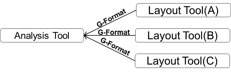
Figure 9 —Example of exchanging layout data with G-Format
N-Format
The purpose of N-Format is to unify the notation of the netlist that is used to design the printed circuit board and the package, where “the netlist” means the connectivity information between parts mounted on a printed circuit board or package. N-Format conforms to Verilog hardware description language (HDL) (IEEE Std 1364) and adds keywords to identify power and ground nets. Unifying notation of the netlist makes it possible to exchange the netlist seamlessly between circuit design tools and layout tools. For example, when the circuit designer orders the board design from the board designers, the circuit designers should exchange the netlist. If the netlist is represented using several notations, there is a risk that human error may occur when entering the connectivity between parts into the design tools. However, by using the unified notation for netlist, it is possible to prevent human errors when setting up the design tools because all design tools can set up the connectivity between parts by supporting only one notation for the netlist file. Figure 10 shows an example of design flow using the N-Format file. The circuit modification is exchanged using N-Format.
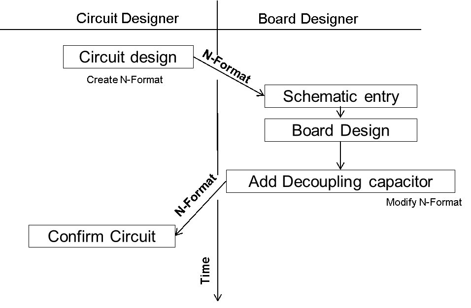
Figure 10 — Example of design flow with N-Format
M-Format
LPB Format files are continuously updated in accordance with the design progress. The purpose of M‑Format is to manage the version of each file to prevent errors when exchanging LPB Format files.