
About Us
JEITA Semiconductor design technical committee is aiming for merging the design technology of “semiconductor” and “system”.
While invention and sales of electronic devices continue to happen, it is important to sometimes merge the technologies in the supply chain and plan out the product project. In order for this to happen, it is significant to distribute each individual technology. The IEEE Standard Format for LSI Package Board (LPB) Interoperable Design is an international standard that gives a role to represent the distribution of technologies. The Semiconductor design technical committee will base this international standard to research and develop the system design to attain the goal “Use of semiconductor in the system design” “Incorporate the requirements and constraints of the system into the semiconductor”. Through this activity, we will contribute to develop the semiconductor industry and electronics industry.
What is LPB?
LPB is the interoperable design of LSI · package board. LPB aims to work closely 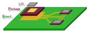 together to finish competitive product design quickly.
IEC 63055/IEEE2401-2015
IEC 63055/IEEE2401-2015 is an international standard that we are promoting t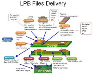 o distribute necessary information and design results related to LPB. Purchase from here.
Organization
Semiconductor & System Design Technical Committee
The development and utilization of this standard are inherited by the JEITA Semiconductor Standardization Committee - Semiconductor & System Technical Committee, which was newly established in April 2017
In order to realize our purpose, we have established the following working groups.
International Standardization and Planning Working Group
This working group plans international standards and steering the committees.
LPB Interface Working Group
This working group spreads and enhances IEC 63055 / IEEE 2401-2015.
LPB modeling Working Group
This working group researches the simulation model and offers the standardization.
Back ground
- The interaction of the components (electronic parts, wiring, inter-layer, etc.) on the electronic device becomes complicated by high density, high quality, high performance.
- The following problem has occurred due to the fact that the format of design information is not unified for each component
- Complicated design work; Development period / cost increase
- Difficult to gather necessary information
- Supply chain connection is weak
- Information of each component is mutually shared, and an optimum solution must be found.